Moore’s Law be damned. IBM announced today (Oct. 1) that it had overcome one of the major hurdles preventing carbon nanotubes from being used as transistors for computer chips. It could mean the end of the silicon computer chip.
Carbon nanotubes are, as their name somewhat suggestions, thin rolled-up sheets of carbon, only one atom thick. These tiny tubes display all sorts of useful characteristics, such as being super strong, super insulating, and being great, reliable semiconductors. That makes them a great material for computer chips, as they process the ability, like silicon, to switch between having electrical current flow through them or not.
They’re also considerably smaller than the smallest silicon transistors on the market. Intel’s current chips are 10 nanometers wide, roughly the length of a few strands of DNA, and the company is struggling to shrink its technology much smaller. IBM, however, announced in July that it had managed to build a silicon transistor just 7 nm wide, and was looking at how how to make one even smaller. But a single carbon nanotube is only about 1 nm wide, meaning if it were possible to wrangle enough of them together—millions or billions on a single chip—it’d be possible to have computer chips considerably faster than anything currently available.
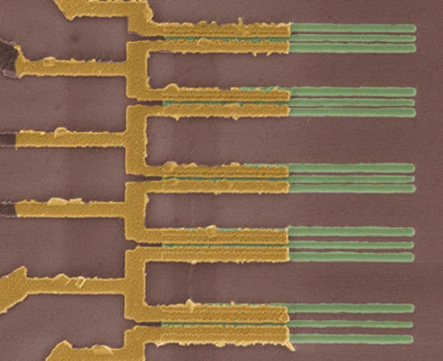
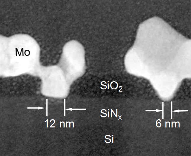
The big hurdle that IBM has cleared is figuring out how to connect nanotubes together efficiently. In a paper published in the Oct. 2 edition of research journal Science, IBM’s research team outlined how to scale down the contact size—the piece of material that connects two semiconductors together—to the same scale that they have managed to produce carbon nanotubes
While scientists have been forging ahead to figure out how to make transistors smaller and smaller, there had not been an effective solution to connect carbon nanotubes together at a scale smaller than 10 nm. IBM’s researchers have figured out a process to connect carbon nanotubes together at their ends, essentially welding (on the atomic scale, no less) the the metal molybdenum to the nanotubes to fuse them together. Researchers found that molybdenum acts as an effective contact material between nanotubes which doesn’t effect how well the tubes can conduct electricity, effectively showing that millions of tubes could be connected together to make computer chips.
Shu-Jen Han, a manager on IBM’s carbon nanotubes research at its research facility in Yorktown Heights, NY, told Quartz that this announcement is a breakthrough that “definitely shows the possibility for carbon nanotube chips” in the future. While there are still a few other obstacles in the path of carbon nanotube chips, Han said that the team has “filled in the one of last missing pieces” in proving that this technology can be developed on the scale needed to make tomorrow’s computer chips.

Still, there are a few more hurdles. First, there’s the way they’re currently developed, or “grown.” There are a few different methods, but they all essentially involve reacting carbon some states—such as graphene, or a hydrocarbon gas—with a catalyst to build up the tubes. When they are grown, two types of nanotubes are formed—metallic and semiconducting—and we only need the semiconducting ones for chips. IBM says it’s developed a process that ensures 99.99% of the tubes it can grow are semiconducting, but that it wants to add a few more nines onto that number before it’s comfortable in saying it’s figured out the growing process.
Then there’s the issue of getting the tubes to line up uniformly so they’re all acting the same way at the same time. Silicon chips are cut out out of near-perfect wafers of silicon in a process that was actually first patented by IBM in 1965. IBM compares this to carving a statue out of marble. With carbon nanotubes, there’s no such process available—scientists have to figure out how to take the tubes they’ve grown and arrange them as perfectly as they could on a wafer—like taking marble dust and figuring how to make that into a statue.

But Han and IBM are confident that they will be able to figure these issues out—they have teams working on each of these individual problems in the near future. And if they’re able to, we could see vastly smaller computer chips with some pretty unique features. Han says the chips would obviously be faster (as the tubes are smaller than silicon transistors, you can fit a greater number of them in the same amount of space), but they’ll also consume a lot less power than silicon chips. This would be a boon for power-hungry modern electronics like smartphones, but also big data centers. “Cooling data centers is an art,” Han said, “And if you can save power there, it’ll definitely mean a lot.”
Han also suggested that future carbon nanotube chips wouldn’t necessarily have to live on a hard wafer like silicon chips do. As carbon nanotubes are strong and flexible, the devices they’re built into can be as well, meaning future wearable devices could be as flexible as any other piece of clothing you wear. They would also come in pretty handy for nanobots—the minuscule robots that researchers are developing that could potentially be injected into humans to help fight heart disease or cancer.
While Moore’s Law—the notion that computer processing power doubles every two years—has been stretched to its absolute limits in recent years as we approach the physical limits of silicon, carbon nanotubes could extend the premise for generations of chips. But first, we’ll need to figure out how to turn marble dust into statues.
